Honeywell 13MM Pressure Sensor Boosts Semiconductor Yield and Purity
AutoControl GlobalAutoControl Global April 13, 2026Honeywell 13MM Pressure Sensor: Advancing Ultra-High Purity in Semiconductor Fabrication
Innovation Drives Precision in High-Tech Manufacturing
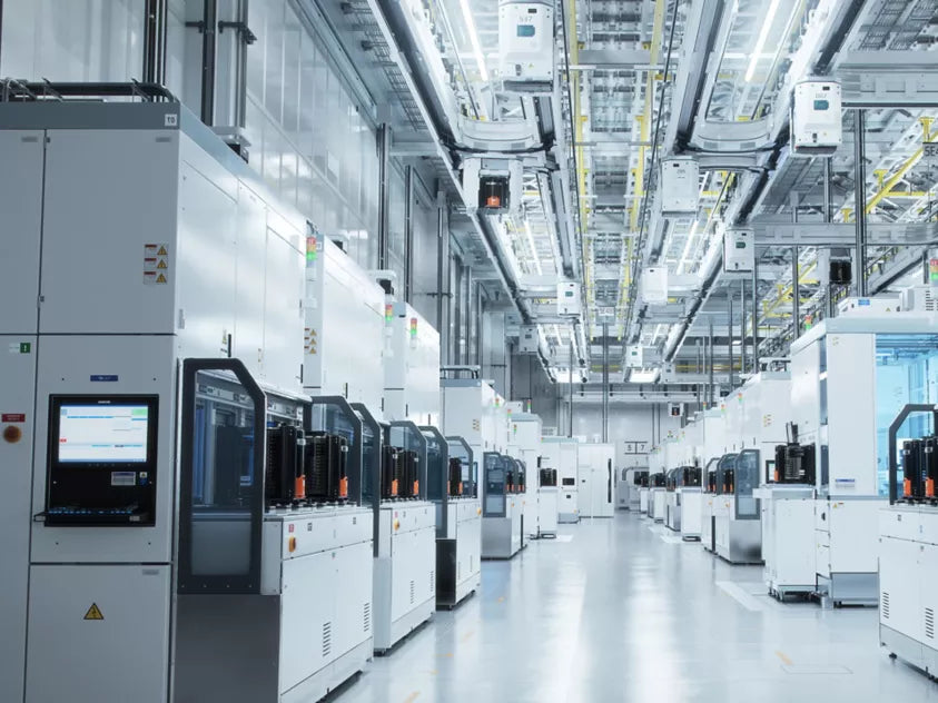
Honeywell recently launched the 13MM Pressure Sensor, specifically engineered for the rigorous demands of cleanroom environments. This solution targets high-purity industries like semiconductor production. In this sector, even microscopic contaminants can destroy entire batches of wafers. Therefore, maintaining a sterile environment is a mechanical necessity for success. This technology highlights a shift toward more specialized industrial automation components that prioritize material integrity alongside measurement accuracy.
Minimizing Offset Drift in Vacuum Environments
Standard pressure sensors often face "drift" issues during long-term vacuum operations. This phenomenon leads to inaccurate data and necessitates frequent recalibration. However, Honeywell’s 13MM Pressure Sensor maintains high accuracy under extreme pressure and temperature conditions. It minimizes offset drift significantly. As a result, equipment operators can maintain precise wafer specifications. This reliability reduces the risk of defects during the critical gas-handling phases of fabrication.
Adhering to Stringent SEMI F20 Industry Standards
The 13MM Pressure Sensor complies with the SEMI F20 standard. This regulation dictates strict metal composition and surface roughness requirements for semiconductor hardware. By meeting these benchmarks, the sensor ensures that its own surfaces do not introduce impurities. Consequently, businesses see an improvement in overall yield and a reduction in expensive wafer scrap. In my view, adhering to such niche standards is what separates professional-grade sensing solutions from generic factory automation tools.
Versatile Applications Across Ultra-High Purity Sectors
While the semiconductor industry is the primary beneficiary, this sensor offers value to other sophisticated sectors. For instance, solar panel and display manufacturing require similar levels of cleanliness. Moreover, the biopharmaceutical and medical equipment industries can utilize this technology to ensure sterile processing. The expansion into food and beverage production shows that ultra-high purity is becoming a universal standard across the broader industrial automation landscape.
Expert Insight: The Future of Cleanroom Sensing
The introduction of the 13MM Pressure Sensor aligns with the global megatrend of advanced automation. As wafer features shrink to the sub-5nm scale, the margin for error effectively disappears. I believe that the future of the semiconductor sector depends on "silent" infrastructure like these sensors. They must work perfectly without becoming part of the chemistry. Honeywell’s focus on material science, rather than just electronic output, reflects a deep understanding of E-E-A-T principles in technical engineering.
Solution Scenarios and Industrial Applications
-
Wafer Fabrication: Monitoring specialized gases during etching and deposition phases to ensure feature precision.
-
Biopharmaceutical Filtration: Maintaining pressure balance in sterile environments without risking metallic contamination.
-
Advanced Optics Production: Controlling vacuum levels during the coating of high-precision lenses and mirrors.
-
Solar Cell Layering: Managing high-temperature gas flows to improve the efficiency of photovoltaic cells.