Server-Grade AOI Architecture Redefines Industrial Edge AI
AutoControl GlobalAutoControl Global June 10, 2026Next-Gen Industrial Automation: How Server-Grade Architecture Redefines High-End Automated Optical Inspection
Advanced semiconductor manufacturing demands unprecedented levels of precision, speed, and reliability from modern factory automation systems. As wafers shrink below the 2nm threshold, traditional machine vision infrastructure struggles to keep pace with soaring processing demands. Consequently, high-end Automated Optical Inspection (AOI) has emerged as a critical pillar of industrial Edge AI systems. This technology enables micro-particle identification and complex 3D structure reconstruction for high-density packages like Chip-on-Wafer-on-Substrate (CoWoS). To maintain maximum throughput, the industry must transition toward next-generation computing architectures.
The Limitations of Traditional Control Systems in Modern Vision Applications
Standard industrial PCs (IPCs) have long served as the backbone of factory automation and basic machine control. However, these legacy systems suffer from insufficient PCIe lanes and narrow communication bandwidth. This infrastructure limitation frequently causes data bottlenecks and system instability during multi-camera inspection cycles. While a typical DCS or PLC manages standard operational data efficiently, high-end AOI systems generate massive data streams. Therefore, engineers require a more robust processing architecture to prevent costly packet loss and localized hardware failures.
Overcoming Bandwidth Bottlenecks with Server-Grade Computing Architecture
To achieve sub-2nm precision, advanced inspection platforms require ultra-high bandwidth exceeding 100 Gbps per system. Fortunately, the integration of server-grade computing architecture effectively solves the data throughput limitations of legacy hardware. Modern systems leverage high-speed protocols like CoaXPress and CoaXPress-over-Fiber (CXPoF) to manage heavy multi-camera workloads. Moreover, this approach provides engineers with over 100 PCIe lanes and multiple expansion slots. As a result, facilities can consolidate multiple processing tasks into a single, compact hardware footprint.
Addressing Power Stability and Thermal Management Challenges
Transitioning to high-performance hardware introduces significant power consumption and thermal challenges into the control room. Server-grade systems consume considerable base power, while high-end GPUs can trigger massive instantaneous power peaks. These sudden spikes often cause voltage drops, digital signal distortion, and unexpected system reboots. To eliminate these critical risks, system designers must adhere strictly to the latest PCIe Gen 5.0 ATX 3.1 specifications. Additionally, implementing dense 4U chassis layouts with optimized airflow prevents thermal throttling during intense AI workloads.
Technical Analysis of the ADLINK ISB-W890 Platform
The ADLINK ISB-W890 Server-Grade Platform delivers a specialized hardware solution designed for intense data processing pipelines. As a core component of the AXE family, this machine features 11 PCIe expansion slots supporting 128 total PCIe lanes. Furthermore, all PCIe lanes route directly to the CPU to minimize transmission latency during real-time image analysis. Full compliance with the ATX 3.1 specification ensures total system stability during maximum GPU computing loads. The platform also offers extensive connectivity, including multiple MCIO groups, 10x USB ports, and 5x COM ports.
Author Perspective: The Strategic Role of DMA in Cognitive Inspection
From an automation engineering perspective, the true breakthrough of the ISB-W890 lies in its optimized memory architecture. By utilizing dedicated Direct Memory Access (DMA) engines, pre-validated frame grabbers can bypass the CPU entirely. This hardware configuration writes raw image data directly into the system memory or the active GPU. Consequently, this complete CPU offloading frees up critical processing cycles exclusively for complex defect classification algorithms. In my view, this architecture bridges the traditional gap between high-speed physical inspection and cognitive Edge AI analysis.
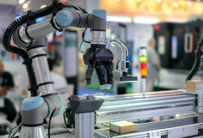
Industrial Automation Application Scenario: Real-Time Advanced Packaging Inspection
The following sequence illustrates how the ADLINK ISB-W890 functions within a modern, automated semiconductor packaging line:
- Multi-Axis Acquisition: High-speed CoaXPress cameras capture simultaneous, six-sided 3D images of a CoWoS wafer assembly during transport.
- Zero-Latency Transfer: The Euresys Coaxlink frame grabber routes the massive 100 Gbps data stream directly to the GPU via DMA engines.
- Edge AI Processing: Three full-size x16 GPU cards run parallel machine learning models to detect micro-bump misalignments in real time.
- Closed-Loop Feedback: The ISB-W890 instantly transmits coordinates of any detected defects to the master PLC over the factory network.
- Automated Sorting: The local control system automatically reroutes compromised chiplets to a secondary rework station without stopping the primary production line.